2023
[33]. “Synergizing Plasmonic Au Nanocages with 2D MoS2 Nanosheets for Significant Enhancement in Photocatalytic Hydrogen Evolution”
R. Peng, X. Ma, Z. D. Hood, A. Boulesbaa, A. Puretzky, J. Tong, and Z. Wu,
J. Mater. Chem. A, (2023), doi: 10.1039/D3TA1657A
[32]. “Fluorescence in Colloidal Solutions: Scattering vs Physicochemical Effects on Line Shape”
Radha Ranganathan, Luis Manuel Davila Muñoz, Miroslav Peric, and A. Boulesbaa
Spectrochimica Acta Part A: Molecular and Biomolecular Spectroscopy, 291 (2023), doi: 10.1016/j.saa.2023.122356
2022
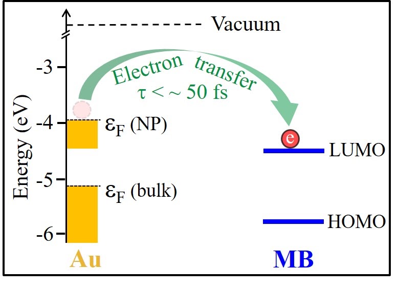
[31] "Ultrafast Electron Transfer at the Interface of Gold Nanoparticles and Methylene Blue Molecular Adsorbates"
D. Contreras, J. M. Yuson, Z. E. Eroglu, P. Bahrami, H. Sadeghi Hadad zavareh, and A. Boulesbaa
Phys. Chem. Chem. Phys. (2022), DOI: 10.1039/D2CP02568J
Abstract: Due to their unique property of possessing localized surface plasmon resonance (LSPR), metal nanoparticles (MNPs) have drastically impacted many applications. For instance, local field enhancement through LSPRs and plasmonic hot electron transfer are known to enhance the efficiency of MNP-based photoreactions. Here, we report on the ultrafast electron transfer from gold nanoparticle (Au-NPs) to methylene blue (MB) molecular adsorbate using femtosecond pump-probe and steady-state absorption and emission spectroscopy techniques. Although the energy band alignment of the interface allows both dipole-dipole Förster resonance energy transfer (FRET) and charge transfer, because the MB emission intensity at the Au-NPs/MB nanocomposite decreased by a factor of ~ 3.6, the FRET process was ruled out. Selective excitation of LSPRs at the Au-NPs/MB nanocomposite sample in pump-probe experiments led to the formation of the MB ground-state depletion and an induced absorption at wavelengths shorter than ~ 500 nm, which was attributed to the shoulder of the MB- anion absorption. Furthermore, despite the fact that the concentration of Au-NPs in the nanocomposite sample is the same as that in the Au-NPs solution, the initial intensity of the LSPR depletion signal was about six times weaker than that in the Au-NPs sample. These observations suggest that electron transfer from excited Au-NPs to MB adsorbates took place on a time-scale that is shorter than the ~ 50 fs experimental temporal resolution.
[30]. “Dynamics of exciton formation, recombination, and trapping in monolayers of 2D-TMD materials ”
J. M. Yuson, D. Contreras, M. Achterman, E. Jung, A. Boulesbaa
Proc. SPIE 11990, Nanoscale and Quantum Materials: From Synthesis and Laser Processing to Applications 2022, 1199005 (4 March 2022); doi.org/10.1117/12.2630804
Abstract: The optical and electrical properties of two-dimensional transition metal dichalcogenide materials (2D-TMDs) are determined by their exciton dynamics. When the thickness of these materials is thinned down to a single layer, the spatial confinement makes the impact of exciton dynamics on the functionality of 2D-TMD-based devices even more important. Here, we present an investigation of the dynamics of formation and decay of the lowest excitons 2D-TMD monolayers. Excitation energy-dependent transient absorption studies indicated that the exciton formation time increases linearly from ~150 fs upon resonant excitation to ~500 fs following excitation that is ~1.1 eV above the bandgap. This dependence is attributed to the time it takes highly excited electrons in the conduction band (CB) to relax to the CB minimum (CBM) and contribute to the formation of the XA exciton. Additionally, excitation energy dependent studies suggested that the exciton average lifetime increases from ~10 ps in the case of resonant excitation to ~50 ps following excitation well above the band-gap. Furthermore, studies of the dependence of exciton dynamics on the excitation density suggested that exciton decay in these materials is dominated by defect-assisted recombination (DAR).
2021
[29]. “Prospects of Nanomaterials in Medicinal Photo-Physical-Chemistry ”
P. Bahrami, D. Contreras, and A. Boulesbaa
Organic & Medicinal Chem IJ, 10 (5), (2021), OMCIJ.MS.ID.555797
Abstract: During the last few decades, nanotechnology and lasers have made their way into many applications, including the medical field. For instance, noble metal nanoparticles (MNPs) and semiconductor quantum dots (QDs) have been used in medical diagnostics, photothermal therapy (PTT), drug delivery, and biolabeling. In a PTT process, the tumor area is exposed to an infrared laser with a frequency selected accordingly with respect to the localized surface plasmon resonance (LSPR) of the MNPs injected around the tumor; the local increase in the temperature of MNPs may lead to the burning of the surrounding tumor cells. Although several research efforts have targeted these concepts, most of the investigations were limited to the examination of the efficiency of the overall process and its dependence on the physical and chemical properties of MNPs and their biofunctionalization. Here, we present an opinion to shed light on the fundamental photophysical and photochemical aspects of the nanomaterials-based PTT process, which may open new horizons for the incorporation of nanomaterials in the medical field.
[28]. “Filling Exciton Trap-States in Two-Dimensional Tungsten Disulfide (WS2) and Diselenide (WSe2) Monolayers”
Z. E. Eroglu, D. Contreras, P. Bahrami, N. Azam, M. Mahjouri-Samani, and A. Boulesbaa
Nanomaterials, 11 (2021), 770
Abstract: Two-dimensional transition metal dichalcogenides (2D-TMDs) hold a great potential to platform future flexible optoelectronics. The beating hearts of these materials are their excitons known as XA and XB, which arise from transitions between spin-orbit split (SOS) levels in the conduction and valence bands at the K-point. The functionality of 2D-TMD-based devices is determined by the dynamics of these excitons. One of the most consequential channels of exciton decay on the device functionality is the defect-assisted recombination (DAR). Here, we employ steady-state absorption and emission spectroscopies, and pump density-dependent femtosecond transient absorption spectroscopy to report on the effect of DAR on the lifetime of excitons in monolayers of tungsten disulfide (2D-WS2) and diselenide (2D-WSe2). These pump-probe measurements suggested that while exciton decay dynamics in both monolayers are driven by DAR, in 2D-WS2, defect states near the XB exciton fill up before those near the XA exciton. However, in the 2D-WSe2 monolayer, the defect states fill up similarly. Understanding the contribution of DAR on the lifetime of excitons and the partition of this decay channel between XA and XB excitons may open new horizons for the incorporation of 2D-TMD materials in future optoelectronics.
2020
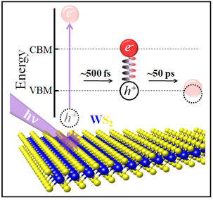
"Ultrafast dynamics of exciton formation and decay in two-dimensional tungsten disulfide (2D-WS2) monolayers"
Z. Ezgi Eroglu, O. Comegys, L. S. Quintanar, N. Azam, S. Elafandi, M. Mahjouri-Samani, A. Boulesbaa
Physical Chemistry-Chemical Physics, 22 (2020), 17385-17393
Abstract. Excitons in two-dimensional transition metal dichalcogenide monolayers (2D-TMDs) are of essential importance due to their key involvement in 2D-TMD-based applications. For instance, exciton dissociation and exciton radiative recombination are indisponsable processes in photovoltaic and light-emitting devices, respectively. These two processes depend drastically on the photogeneration efficiency and lifetime of excitons. Here, we incorporate femtosecond pump-probe spectroscopy to investigate the ultrafast dynamics of exciton formation and decay in a single crystal of 2D tungsten disulfide (WS2) monolayer. Investigation of the formation dynamics of the lowest exciton (XA) indicated that the formation time linearly increases from ~150 fs upon resonant excitation, to ~500 fs following excitation that is ~1.1 eV above the band-gap. This dependence is attributed to the time it takes highly excited electrons in the conduction band (CB) to relax to the CB minimum (CBM) and contribute to the formation of XA. This is confirmed by infrared measurements of electron intraband relaxation dynamics. Furthermore, pump-probe experiments suggested that the XA ground state depletion recovery dynamics depend on the excitation energy as well. The average recovery time increased from ~10 ps in the case of resonant excitation to ~50 ps following excitation well above the band-gap. Having the ability to control whether generating short-lived or long-lived electron-hole pairs in 2D-TMD monolayers opens a new horizon for the application of these materials. For instance, long-lived electron-hole pairs are appropriate for photovoltaic devices, but short-lived excitons are more beneficial for lasers with ultrashort pulses.
2019
[26]. "Accelerated synthesis of atomically-thin 2D quantum materials by a novel laser-assisted synthesis technique"
N. Azam, Z. Ahmadi, B. Yakupoglu, S. Elafandi, M. Tian, A. Boulesbaa, and M. Mahjouri-Samani
2D Materials, 7 (2019),
Abstract: Two-dimensional (2D) layered materials including transition metal dichalcogenides (TMDCs) have recently been at the heart of the quantum materials and information sciences research due to unusual properties associated with their firmly defined dimensionalities. Many efforts have focused on developing new methods for the accelerated growth and discovery of 2D materials, including physical and chemical vapor deposition techniques. However, the synthesis of these multi-component crystals in the gas phase has been extremely challenging due to complex and uncontrolled gas-phase reactions and flow dynamics. Here, we demonstrate a novel laser-assisted synthesis technique (LAST), which significantly reduces the existing growth complexities and notably accelerates the growth of 2D materials. This approach facilitates the growth of various 2D materials directly from stoichiometric powders by laser vaporization process. We show that directed laser heating allows pressure-independent decoupling of the growth and evaporation kinetics enabling the use of stoichiometric powder as precursors for the growth of high-quality 2D materials including MoS2, MoSe2, WSe2, and WS2. A comprehensive experimental study was conducted to identify the system behavior, including the evaporation and growth parameters as well as the process-property relationships. This method presents a general yet simple approach for accelerating the discovery of emerging quantum materials.
2018
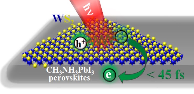
[25] "Ultrafast Exciton Dissociation at the 2D-Ws2 Monolayer/Perovskite Interface "
J. Bauer, L. S. Quintanar, K. Wang, A. A. Puretzky, K. Xiao, D. B. Geohegan, and A. Boulesbaa
J. Phys. Chem. C, 1122 (2018), 28910–28917
Abstract: In order for an excitonic photovoltaic (PV) device to perform efficiently, photogenerated excitons in the charge donor need to be dissociated through charge transfer (CT) to the acceptor rapidly after their photogeneration, and remain separated for a longer time to allow the collection of charges. To improve the efficiency of these steps, several combination of materials have been examined. Due to their excellent optical properties, two-dimensional transition metal dichalcogenides (2D-TMDs) have recently been explored. Another promising class of materials to platform efficient PVs is organic-inorganic perovskites. Here, we report on the ultrafast exciton dissociation through electron transfer from a 2D tungsten disulfide (WS2) monolayer to a thin layer of methylammonium lead iodide (CH3NH3PbI3) perovskites. Photoluminescence (PL) measurements showed that when the 2D-WS2 monolayer was covered with perovskites, its emission completely quenched, suggesting that the CT process is highly efficient. Despite that pump-probe spectroscopy measurements were carried out with a ~ 45 fs temporal resolution, the CT dynamics were not captured. A comparison of the ultrafast dynamics of the two band-edge excitons of the charge donor (2D-WS2) suggested that electron transfer is the dominant pathway of CT. Furthermore, these pump-probe measurements indicated that a small fraction of transferred electrons remained in the perovskites up to almost 2 ns. These findings may open a new horizon for understanding the dissociation of photogenerated excitons in 2D-TMD through hybridization with other class of nanomaterials.
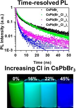
[24] "Ultrafast Spectral Dynamics of CsPb(BrxCl1–x)3 Mixed-Halide Nanocrystals"
N. Soetan, A. Puretzky, K. Reid, A. Boulesbaa, H. F. Zarick, A. Hunt, O. Rosenthal, D. B. Geohegan, and R. Bardhan
ACS Photonics, 5 (2018), 3575-3583
Abstract: In this work we investigated the spectral dynamics of cesium lead mixed-halide, CsPb(BrxCl1−x)3 perovskite nanocrystals probed with complementary spectral techniques: time-resolved photoluminescence and transient absorption spectroscopy. Mixed-halide perovskite nanocrystals were synthesized via a hot-injection method followed by anion exchange reactions. Our results show that increased Cl content in perovskite nanocrystals (a) diminished the photoluminescence quantum yield and gave rise to rapid radiative recombination of carriers; (b) resulted in rapid thermalization of hot carriers and low carrier temperatures, which suggests weaker hot-phonon bottleneck and Burstein−Moss effects; (c) decreased the bandgap renormalization energy, which suggests high exciton binding energy and poor charge extraction in Cl substituted perovskite nanocrystals; and (d) increased the number of carriers undergoing Auger losses, where Auger processes dominate over trapassisted recombination. These findings provide a generalized framework to guide researchers as to when mixed-halide perovskite nanocrystals would be useful for optoelectronic technologies and when they would be detrimental to device performance.

[23]. "Laser Synthesis, Processing, and Spectroscopy of Atomically-Thin Two Dimensional Materials"
Advances in the Application of Lasers in Materials Science, Springer, Cham 1-37 (2018)
D. B. Geohegan, A. A. Puretzky, A. Boulesbaa, G. Duscher, Gyula. Eres, X. Li, L. Liang, M. Mahjouri-Samani, C. Rouleau, W. Tennyson, M. Tian, K. Wang, K. Xiao, M. Yoon
Abstract: Atomically-thin two-dimensional (2D) materials display widely varying electronic and vibronic properties compared to their bulk counterparts. Laser interactions with 2D materials are central to their development. Here, we attempt to overview recent progress and define the current challenges in the broad range of laser interactions involved in the synthesis, processing, and optical characterization of 2D materials as the field has emerged from graphene and h-BN to encompass a multitude of other atomically-thin semiconducting, superconducting, thermoelectric, etc. 2D materials as “building blocks” for future energy applications and devices. Here, we first focus on challenges in the synthesis and processing of mainly semiconducting 2D layers for optoelectronics, and the advantages offered by non-equilibrium laser processing. Then, we review the optical characterization techniques that are being developed to serve as remote probes of their electronic and vibronic properties, as well as their structure, stacking, and atomistic alignment. Together, examples will be shown how these developments are already being merged to fulfill the promise for tailored synthesis and assembly of these exquisite materials with real-time in situ control of structure and optoelectronic properties.
2017
[22]. “Synthesis and Photoluminescence Properties of 2D Phenethylammonium Lead Bromide Perovskite Nanocrystals”
R. Guo, Z. Zhu, A. Boulesbaa, F. Hao, A. Puretzky, K. Xiao, J. Bao, Y. Yao, W. Li
Small Methods, 1 (2017), 1700245
Abstract: Organic–inorganic hybrid perovskites have emerged as promising optoelectronic materials for applications in photovoltaic and optoelectronic devices. Particularly, 2D layer‐structured hybrid perovskites are of great interest due to their remarkable optical and electrical properties, which can be easily tuned by selecting suitable organic and inorganic moieties during the material synthesis. Here, the solution‐phase growth of a large square‐shaped single‐crystalline 2D hybrid perovskite, phenethylammonium lead bromide (C6H5C2H4NH3)2PbBr4 (PEPB), with thickness as few as 3 unit cell layers is demonstrated. Compared to bulk crystals, the 2D PEPB nanocrystals show a major blueshifted photoluminescence (PL) peak at 409 nm indicating an increase in bandgap of 40 meV. Besides the major peak, two new PL peaks located at 480 and 525 nm are observed from the hybrid perovskite nanocrystals. PEPB nanocrystals with different thicknesses show different colors, which can be used to estimate the thickness of the nanocrystals. Time‐resolved reflectance spectroscopy is used to investigate the exciton dynamics, which exhibits a biexponential decay with an amplitude‐weighted lifetime of 16.7 ps. The high‐quality 2D (C6H5C2H4NH3)2PbBr4 nanocrystals are expected to have high PL quantum efficiency and potential applications for light‐emitting devices.
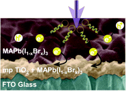
[21]. “Bromine Substitution Improves Excited-State Dynamics in Mesoporous Mixed Halide Perovskite Films”
E. M. Talbert, H. F. Zarick, A. Boulesbaa, N. Soetan, A. A. Puretzky, D. B. Geohegan, and R. Bardhan
Nanoscale, 9 (2017), 12005-12013
Abstract: In this study, ultrafast transient absorption spectroscopy (TAS) is utilized to examine the excited-state dynamics in methylammonium lead iodide/bromide (MAPb(I1−xBrx)3) perovskites as a function of bromide content. TAS spectral behavior reveals characteristic lifetimes for thermalization, recombination, and charge carrier injection of MAPb(I1−xBrx)3 from x = 0 to 0.3 infiltrated in mesoporous titania films. Carrier recombination and charge injection lifetimes demonstrated a discernable increase with Br content likely because high carrier populations are supported by the higher density of vacant electronic states in mixed-halide perovskites due to the increased capacity of the conduction band. However, we observe for the first time that carrier thermalization lifetimes significantly decrease with increasing Br. This suggests that the shift in crystal structure from tetragonal towards pseudocubic accelerates carrier cooling, resulting in the relief of the hot phonon bottleneck. Furthermore, the stabilized MAPb(I1−xBrx)3 samples exhibit a lower Burstein–Moss shift of 0.07–0.08 eV compared to pure MAPbI3(0.12 eV). Our results provide evidence that Br inclusion contributes to a broadening of the parabolic conduction band and to improvement in electron–phonon coupling and phonon propagation in the lattice.
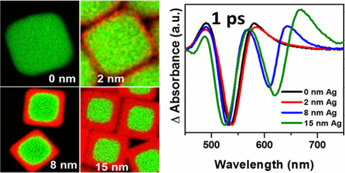
[20]. "Ultrafast Excited-State Dynamics in Shape- and CompositionControlled Gold−Silver Bimetallic Nanostructures "
H. F. Zarick, A. Boulesbaa, E. M. Talbert, A. Puretzky, D. Geohegan, and R. Bardhan
J. Phys. Chem. C, 121 (2017), 4540–4547
Abstract: In this work, we have examined the ultrafast dynamics of shape- and composition-controlled bimetallic Au/ Ag core/shell nanostructures with transient absorption spectroscopy (TAS) as a function of Ag layer thickness (0−15 nm) and pump excitation fluence (50−500 nJ/pulse). Our synthesis approach generated both bimetallic nanocubes and nanopyramids with distinct dipolar plasmon resonances and plasmon dephasing behavior at the resonance. Lifetimes obtained from TAS at low powers (50 nJ/pulse) demonstrated minimal dependence on the Ag layer thickness, whereas at high power (500 nJ/pulse) a rise in electron−phonon coupling lifetime (τ1) was observed with increasing Ag shell thickness for both nanocubes and nanopyramids. This is attributable to the stronger absorption of the 400 nm pump pulse with higher Ag content, which induced higher electron temperatures. The phonon−phonon scattering lifetime (τ2) also rises with increasing Ag layer, contributed both by the increasing size of the Au/Ag nanostructures as well as by surface chemistry effects. Further, we observed that even the thinnest, 2 nm, Ag shell strongly impacts both τ1 and τ2 at high power despite minimal change in overall size, indicating that the nanostructure composition also strongly impacts the thermalization temperature following absorption of 400 nm light. We also observed a shape-dependent trend at high power, where τ2 increased for the nanopyramids with increasing Ag shell thickness and nanostructure size, but bimetallic nanocubes demonstrated an unexpected decrease in τ2 for the thickest, 15 nm, Ag shell. This was attributed to the larger number of corners and edges in the nanocubes relative to the nanopyramids.
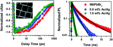
[19]. “Ultrafast Carrier Dynamics in Bimetallic Nanostructures-Enhanced Methylammonium Lead Bromide Perovskites”
H. F. Zarick, A. Boulesbaa, A. A. Puretzky, E. M. Talbert, D. B. Geohegan, R. Bardhan
Nanoscale, 9 (2017), 1475-1483
Abstract: In this work, we examine the impact of hybrid bimetallic Au/Ag core/shell nanostructures on the carrier dynamics of methylammonium lead tribromide (MAPbBr3) mesoporous perovskite solar cells (PSCs). Plasmon-enhanced PSCs incorporated with Au/Ag nanostructures demonstrated improved light harvesting and increased power conversion efficiency by 26% relative to reference devices. Two complementary spectral techniques, transient absorption spectroscopy (TAS) and time-resolved photoluminescence (trPL), were employed to gain a mechanistic understanding of plasmonic enhancement processes. TAS revealed a decrease in the photobleach formation time, which suggests that the nanostructures improve hot carrier thermalization to an equilibrium distribution, relieving hot phonon bottleneck in MAPbBr3 perovskites. TAS also showed a decrease in carrier decay lifetimes, indicating that nanostructures enhance photoinduced carrier generation and promote efficient electron injection into TiO2 prior to bulk recombination. Furthermore, nanostructure-incorporated perovskite films demonstrated quenching in steady-state PL and decreases in trPL carrier lifetimes, providing further evidence of improved carrier injection in plasmon-enhanced mesoporous PSCs.
2016
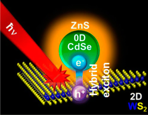
[18]. “Ultrafast Charge Transfer and Formation of Hybrid Excitons at 2D/0D Heterostructures”
A. Boulesbaa, K. Wang, M. Mahjouri-Samani, M. Tian, A. Puretzky, I. Ivanov, C. Rouleau, K. Xiao, B. Sumpter and D. Geohegan
J. Am. Chem. Soc., 138 (2016), 14713-14719
Abstract: Photoinduced interfacial charge transfer is at the heart of many applications, including photovoltaics, photocatalysis, and photodetection. With the emergence of a new class of semiconductors, i.e., monolayer two-dimensional transition metal dichalcogenides (2D-TMDs), charge transfer at the 2D/2D heterojunctions has attracted several efforts due to the remarkable optical and electrical properties of 2D-TMDs. Unfortunately, in 2D/2D heterojunctions, for a given combination of two materials, the relative energy band alignment and the charge-transfer efficiency are locked. Due to their large variety and broad size tunability, semiconductor quantum dots (0D-QDs) interfaced with 2D-TMDs may become an attractive heterostructure for optoelectronic applications. Here, we incorporate femtosecond pump–probe spectroscopy to reveal the sub-45 fs charge transfer at a 2D/0D heterostructure composed of tungsten disulfide monolayers (2D-WS2) and a single layer of cadmium selenide/zinc sulfide core/shell 0D-QDs. Furthermore, ultrafast dynamics and steady-state measurements suggested that, following electron transfer from the 2D to the 0D, hybrid excitons, wherein the electron resides in the 0D and the hole resides in the 2D-TMD monolayer, are formed with a binding energy on the order of ∼140 meV, which is several times lower than that of tightly bound excitons in 2D-TMDs.
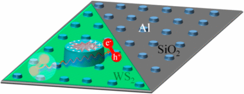
[17]. “Ultrafast Dynamics of Metal Plasmons Induced by 2D Semiconductor Excitons in Hybrid Nanostructure Arrays”
A. Boulesbaa, V. Babicheva, K. Wang, I. Kravchenko, M. W. Lin, M. Mahjouri-Samani, C. Jacobs, A. Puretzky, K. Xiao, I. Ivanov, C. Rouleau, and D. Geohegan
ACS Photonics, 3 (2016), 2389-2395
Abstract: With the advanced progress achieved in the field of nanotechnology, localized surface plasmon resonances are actively considered to improve the efficiency of metal-based photocatalysis, photodetection, and photovoltaics. Here, we report on the exchange of energy and electric charges in a hybrid composed of a two-dimensional tungsten disulfide (2D-WS2) monolayer and an array of aluminum (Al) nanodisks. Femtosecond pump–probe spectroscopy results indicate that within ∼830 fs after photoexcitation of the 2D-WS2 semiconductor energy transfer from the 2D-WS2 excitons excites the plasmons of the Al array. Then, upon the radiative and/or nonradiative damping of these excited plasmons, energy and/or electron transfer back to the 2D-WS2 semiconductor takes place as indicated by an increase in the reflected probe at the 2D-exciton transition energies at later time delays. This simultaneous exchange of energy and charges between the metal and the 2D-WS2 semiconductor resulted in an extension of the average lifetime of the 2D-excitons from ∼15 ps to ∼58 ps in the absence and presence of the Al array, respectively. Furthermore, the indirectly excited plasmons were found to live as long as the 2D-WS2 excitons exist. The demonstrated ability to generate exciton–plasmon coupling in a hybrid nanostructure may open new opportunities for optoelectronic applications such as plasmonic-based photodetection and photocatalysis.
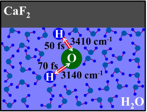
[16]. “Capturing the Ultrafast Vibrational Decoherence of Hydrogen Bonding in Interfacial Water”
A. Boulesbaa, and E. Borguet
J. Phys. Chem. Lett., 7 (2016), 5080-5085
Abstract: Vibrational sum-frequency generation (vSFG) measurements in the frequency and time domains reveal that the interfacial hydrogen bonded OH stretch at the water/calcium fluoride interface is composed of two populations oriented oppositely. The time-resolved vSFG free-induction decay suggested that, whereas the strongly hydrogen bonded OH vibrational stretches, centered near 3140 ± 11 cm–1, are oriented toward bulk water and lose their collective coherence within ∼70 ± 7 fs, the weakly hydrogen bonded OH species, centered near 3410 ± 12 cm–1, are pointed toward the interface and dephase within ∼50 ± 6 fs.

[15]. “In-plane Heterojunctions Enable Multiphasic 2D MoS2 Nanosheets as Efficient Photocatalysts for Hydrogen Evolution from Water Reduction”
R. Peng, L. Liang, Z. Hood, A. Boulesbaa, A. Puretzky, A. Ievlev, J. Come, O. Ovchinnikova, C. Ma, M. Chi, B. Sumpter, Z.Wu
ACS Catal., 6 (2016), 6723–6729
Abstract: Two-dimensional (2D) single-layer MoS2 nanosheets are demonstrated as efficient photocatalysts for hydrogen evolution reaction (HER) from water reduction, thanks to specific in-plane heterojunctions constructed in the MoS2 monolayer. These functional heterojunctions are formed among the different phases of chemically exfoliated MoS2 monolayers: semiconducting 2H, metallic 1T, and quasi-metallic 1T′ phases. The proportion of the three MoS2 phases can be systematically controlled via thermal annealing of the nanosheets. Interestingly, a volcano relationship is observed between the photocatalytic HER activity and the annealing temperature with an optimum activity obtained after annealing at 60 °C. First-principles calculations were integrated with experimental studies to shed light on the role of the multiphases of MoS2 and reveal that optimum photocatalytic HER activity results from the formation of the in-plane heterojunctions between 1T′ MoS2 and 2H MoS2. Importantly, this facilitates not only balanced light absorption and charge generation by the 2H phase, efficient charge separation at the 1T′/2H interface, but also favorable HER over the basal sites of 1T′ MoS2. Our work manifests how the confluence of the optical, electronic and chemical properties of 2D MoS2 monolayers can be fully captured for efficient photocatalytic water reduction.
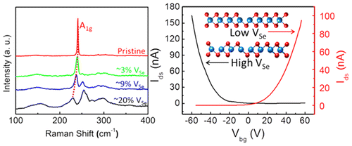
[14]. “Tailoring Vacancies Far Beyond Intrinsic Levels Changes the Carrier Type in Monolayer MoSe2-x Crystals”
M. Mahjouri-Samani, L. Liang, A. Oyedele, M. Tian, N. Cross, M. W. Lin, A. Boulesbaa, C. M. Rouleau, A. Puretzky, K. Xiao, G. Eres, G. Duscher, B. G. Sumpter, and D. B. Geohegan
Nano Letters, 16 (2016), 5213-5220
Abstract: Defect engineering has been a critical step in controlling the transport characteristics of electronic devices, and the ability to create, tune, and annihilate defects is essential to enable the range of next-generation devices. Whereas defect formation has been well-demonstrated in three-dimensional semiconductors, similar exploration of the heterogeneity in atomically thin two-dimensional semiconductors and the link between their atomic structures, defects, and properties has not yet been extensively studied. Here, we demonstrate the growth of MoSe2–x single crystals with selenium (Se) vacancies far beyond intrinsic levels, up to ∼20%, that exhibit a remarkable transition in electrical transport properties from n- to p-type character with increasing Se vacancy concentration. A new defect-activated phonon band at ∼250 cm−1 appears, and the A1g Raman characteristic mode at 240 cm−1 softens toward ∼230 cm−1 which serves as a fingerprint of vacancy concentration in the crystals. We show that post-selenization using pulsed laser evaporated Se atoms can repair Se-vacant sites to nearly recover the properties of the pristine crystals. First-principles calculations reveal the underlying mechanisms for the corresponding vacancy-induced electrical and optical transitions.
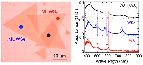
[13]. “Interlayer Coupling in Twisted WSe2/WS2 Bilayer Heterostructures Revealed by Optical Spectroscopy”
K. Wang, B. Huang, M. Tian, F. Ceballos, M. W. Lin, M. Mahjouri-Samani, A. Boulesbaa, A. Puretzky, C. Rouleau, M. Yoon, H. Zhao, K. Xiao, G. Duscher, D. Geohegan
ACS Nano, 10 (2016), 6612-6622
Abstract: van der Waals (vdW) heterostructures are promising building blocks for future ultrathin electronics. Fabricating vdW heterostructures by stamping monolayers at arbitrary angles provides an additional range of flexibility to tailor the resulting properties than could be expected by direct growth. Here, we report fabrication and comprehensive characterizations of WSe2/WS2 bilayer heterojunctions with various twist angles that were synthesized by artificially stacking monolayers of WS2 and WSe2 grown by chemical vapor deposition. After annealing the WSe2/WS2 bilayers, Raman spectroscopy reveals interlayer coupling with the appearance of a mode at 309.4 cm–1that is sensitive to the number of WSe2 layers. This interlayer coupling is associated with substantial quenching of the intralayer photoluminescence. In addition, microabsorption spectroscopy of WSe2/WS2 bilayers revealed spectral broadening and shifts as well as a net ∼10% enhancement in integrated absorption strength across the visible spectrum with respect to the sum of the individual monolayer spectra. The observed broadening of the WSe2 A exciton absorption band in the bilayers suggests fast charge separation between the layers, which was supported by direct femtosecond pump–probe spectroscopy. Density functional calculations of the band structures of the bilayers at different twist angles and interlayer distances found robust type II heterojunctions at all twist angles, and predicted variations in band gap for particular atomistic arrangements. Although interlayer excitons were indicated using femtosecond pump–probe spectroscopy, photoluminescence and absorption spectroscopies did not show any evidence of them, suggesting that the interlayer exciton transition is very weak. However, the interlayer coupling for the WSe2/WS2 bilayer heterojunctions indicated by substantial PL quenching, enhanced absorption, and rapid charge transfer was found to be insensitive to the relative twist angle, indicating that stamping provides a robust approach to realize reliable optoelectronics.

[12]. “Improving Light Harvesting in Dye Sensitized Solar Cells using Hybrid Bimetallic Nanostructures”
H. F. Zarick, O. Hurd, A. Boulesbaa, W. R. Erwin, J. A. Webb, A. Puretzky, D. Geohegan, and R. Bardhan
ACS Photonics, 3 (2016), 385-394
Abstract: In this work we demonstrate improved light trapping in dye-sensitized solar cells (DSSCs) with hybrid bimetallic gold core/silver shell nanostructures. Silica-coated bimetallic nanostructures (Au/Ag/SiO2 NSs) integrated in the active layer of DSSCs resulted in 7.51% power conversion efficiency relative to 5.97% for reference DSSCs, giving rise to 26% enhancement in device performance. DSSC efficiencies were governed by the particle density of Au/Ag/SiO2 NSs with best performing devices utilizing only 0.44 wt % of nanostructures. We performed transient absorption spectroscopy of DSSCs with variable concentrations of Au/Ag/SiO2 NSs and observed an increase in amplitude and decrease in lifetime with increasing particle density relative to reference. We attributed this trend to plasmon resonant energy transfer and population of the singlet excited states of the sensitizer molecules at the optimum concentration of NSs promoting enhanced exciton generation and rapid charge transfer into TiO2.
2015
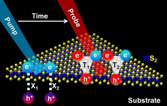
[11]. “Observation of Two Distinct Negative Trions in Tungsten Disulfide Monolayers”
A. Boulesbaa, B. Huang, K. Wang, M. W. Lin, M. Mahjouri-Samani, C. Rouleau, K. Xiao, M. Yoon, B. Sumpter, A. Puretzky, and D. Geohegan
Phys. Rev. B 92, 115443 (2015)
Abstract: Ultrafast pump-probe spectroscopy of two-dimensional tungsten disulfide monolayers (2DWS2) grown on sapphire substrates revealed two transient absorption spectral peaks that are attributed to distinct negative trions at ∼2.02eV (T1) and ∼1.98eV (T2). The dynamics measurements indicate that trion formation by the probe is enabled by photodoped 2D WS2 crystals with electrons remaining after trapping of holes from excitons or free electron-hole pairs at defect sites in the crystal or on the substrate. Dynamics of the characteristic absorption bands of excitons XA and XB at ∼2.03 and ∼2.40eV, respectively, were separately monitored and compared to the photoinduced absorption features. Selective excitation of the lowest exciton level XA using λpump <2.4eV forms only trion T1, implying that the electron remaining from dissociation of exciton XA is involved in the creation of this trion with a binding energy ∼10meV with respect to XA. The absorption peak corresponding to trion T2 appears when λpump <2.4eV, which is just sufficient to excite exciton XB. The dynamics of trion T2formation are found to correlate with the disappearance of the bleach of the XB exciton, indicating the involvement of holes participating in the bleach dynamics of exciton XB. Static electrical-doping photoabsorption measurements confirm the presence of an induced absorption peak similar to that of T2. Since the proposed trion formation process here involves exciton dissociation through hole trapping by defects in the 2D crystal or substrate, this discovery highlights the strong role of defects in defining optical and electrical properties of 2D metal chalcogenides, which is relevant to a broad spectrum of basic science and technological applications.
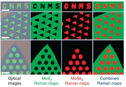
[10]. “Patterned Arrays of Lateral Heterojunctions within Monolayer 2D Semiconductors”
M. Mahjouri-Samani, M. W. Lin, K. Wang, A. Lupini, J. Lee, L. Basile, A. Boulesbaa, C. Rouleau, A. Puretzky, I. Ivanov, K. Xiao, M. Yoon , D. Geohegan
Nature Communications, DOI: 10.1038/ncomms8749 (2015)
Abstract: The formation of semiconductor heterojunctions and their high-density integration are foundations of modern electronics and optoelectronics. To enable two-dimensional crystalline semiconductors as building blocks in next-generation electronics, developing methods to deterministically form lateral heterojunctions is crucial. Here we demonstrate an approach for the formation of lithographically patterned arrays of lateral semiconducting heterojunctions within a single two-dimensional crystal. Electron beam lithography is used to pattern MoSe2 monolayer crystals with SiO2, and the exposed locations are selectively and totally converted to MoS2 using pulsed laser vaporization of sulfur to form MoSe2/MoS2 heterojunctions in predefined patterns. The junctions and conversion process are studied by Raman and photoluminescence spectroscopy, atomically resolved scanning transmission electron microscopy and device characterization. This demonstration of lateral heterojunction arrays within a monolayer crystal is an essential step for the integration of two-dimensional semiconductor building blocks with different electronic and optoelectronic properties for high-density, ultrathin devices.
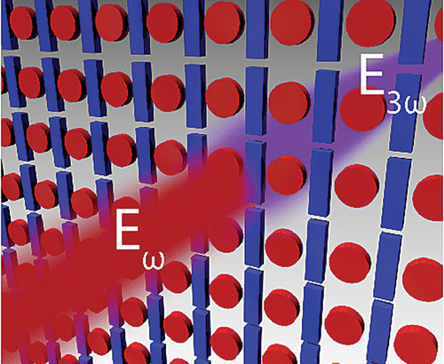
[9]. “Nonlinear Fano-Resonant Dielectric Metasurface”
Y. Yang, W. Wang, A. Boulesbaa, I. I. Kravchenko, D. P. Briggs, A. Puretzky, D. Geohegan, and J. Valentine
Nano Letters, 15 (2015), 7388-7393
Abstract: Strong nonlinear light–matter interaction is highly sought-after for a variety of applications including lasing and all-optical light modulation. Recently, resonant plasmonic structures have been considered promising candidates for enhancing nonlinear optical processes due to their ability to greatly enhance the optical near-field; however, their small mode volumes prevent the inherently large nonlinear susceptibility of the metal from being efficiently exploited. Here, we present an alternative approach that utilizes a Fano-resonant silicon metasurface. The metasurface results in strong near-field enhancement within the volume of the silicon resonator while minimizing two photon absorption. We measure a third harmonic generation enhancement factor of 1.5 × 10⁵ with respect to an unpatterned silicon film and an absolute conversion efficiency of 1.2 × 10⁻⁶ with a peak pump intensity of 3.2 GW cm–2. The enhanced nonlinearity, combined with a sharp linear transmittance spectrum, results in transmission modulation with a modulation depth of 36%. The modulation mechanism is studied by pump–probe experiments.
[8]. “Nonlinear Conversion Using Fano-Resonant All-Dielectric Metasurfaces”
Y. Yang, A. Boulesbaa, I. Kravchenko, D. Briggs, A. Puretzky, D. Geohegan, J. G Valentine
Nonlinear Optics, NTu2B. 5 (2015)
Abstract: We present an experimental demonstration of third harmonic generation from Fano-resonant all-dielectric metasurfaces. The metasurfaces have a conversion enhancement factor of 1.5×10⁵and an absolute conversion efficiency on the order of 10-6.
2014
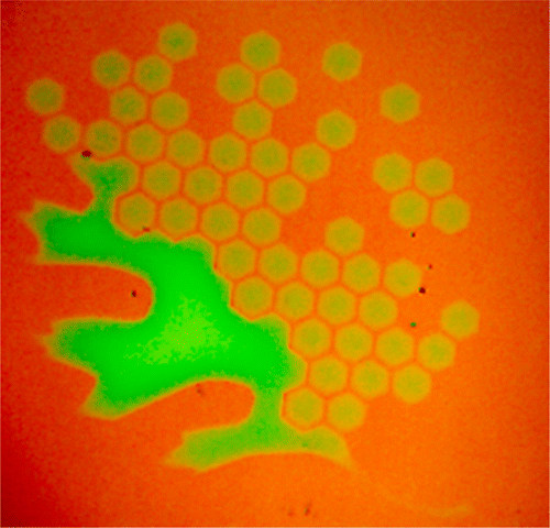
[7]. “Digital Transfer Growth of Patterned 2D Metal Chalcogenides by Confined Nanoparticle Evaporation”
M. Mahjouri-Samani, M. Tian, K. Wang, A. Boulesbaa, C. M. Rouleau, A. A. Puretzky, M. A. McGuire, B. R. Srijanto, K. Xiao, G. Eres, G. Duscher, and D. B. Geohegan
ACS Nano, 8 (2014), 11567-1175
Abstract: Developing methods for the facile synthesis of two-dimensional (2D) metal chalcogenides and other layered materials is crucial for emerging applications in functional devices. Controlling the stoichiometry, number of the layers, crystallite size, growth location, and areal uniformity is challenging in conventional vapor-phase synthesis. Here, we demonstrate a method to control these parameters in the growth of metal chalcogenide (GaSe) and dichalcogenide (MoSe2) 2D crystals by precisely defining the mass and location of the source materials in a confined transfer growth system. A uniform and precise amount of stoichiometric nanoparticles are first synthesized and deposited onto a substrate by pulsed laser deposition (PLD) at room temperature. This sourcesubstrate is then covered with a receiver substrate to form a confined vapor transport growth (VTG) system. By simply heating the source substrate in an inert background gas, a natural temperature gradient is formed that evaporates the confined nanoparticles to grow large, crystalline 2D nanosheets on the cooler receiver substrate, the temperature of which is controlled by the background gas pressure. Large monolayer crystalline domains (∼100 μm lateral sizes) of GaSe and MoSe2 are demonstrated, as well as continuous monolayer films through the deposition of additional precursor materials. This PLD–VTG synthesis and processing method offers a unique approach for the controlled growth of large-area metal chalcogenides with a controlled number of layers in patterned growth locations for optoelectronics and energy related applications.
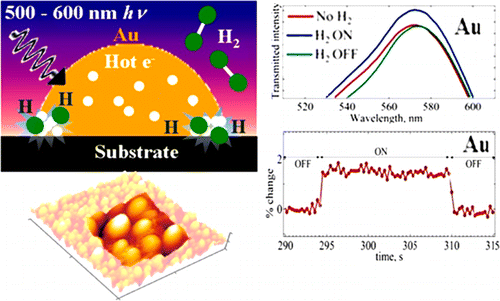
[6]. “Seeing Is Believing: Hot Electron Based Gold Nanoplasmonic Optical Hydrogen Sensor”
D. Sil, K. GilRoy, A. Niaux, A. Boulesbaa, S. Neretina, and E. Borguet
ACS Nano, 8 (2014), 7755-7762
Abstract: We report on the rapid optical detection of gaseous hydrogen using hot electrons generated from resonantly excited substrate-based gold nanohemispheres (Au NHs). We consider hot electron induced H2 dissociation and the subsequent formation of a metastable gold hydride (AuHx) to account for changes in optical transmission. The excitation wavelength was varied to demonstrate a maximum response at the localized surface plasmon resonance (LSPR) wavelength of the AuNHs. Numerical simulations, using the discrete dipole approximation, were employed to corroborate the optical changes associated with the formation of metastable AuHx. Finite time difference domain (FDTD) calculations were also performed to account for the enhanced photocatalytic activity arising due to the confinement of electric fields by the Au NHs. FDTD simulations show that the excitation of the Au NHs plasmon modes generates stronger electric fields at the interface in comparison to a spherical geometry of similar dimensions.
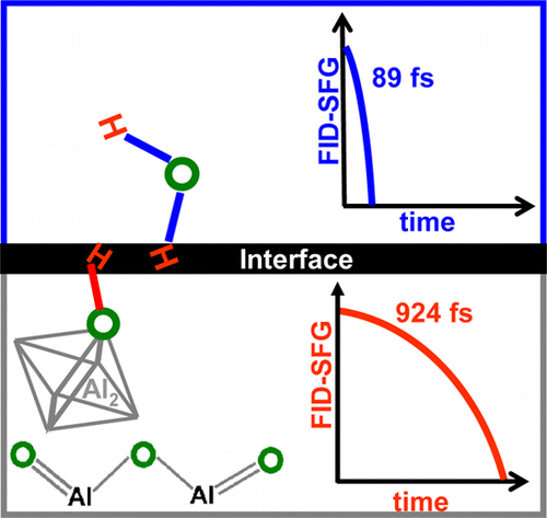
[5]. “Vibrational Dynamics of Interfacial Water by Free Induction Decay Sum-Frequency Generation (FID-SFG) at the Al2O3(1120)/H2O Interface”
A. Boulesbaa and E. Borguet
J. Phys. Chem. Lett., 5 (2014), 528-533
Abstract: The dephasing dynamics of a vibrational coherence may reveal the interactions of chemical functional groups with their environment. To investigate this process at a surface, we employ free induction decay sum frequency generation (FID-SFG) to measure the time that it takes for free OH stretch oscillators at the charged (pH ≈ 13, KOH) interface of alumina/water (Al2O3/H2O) to lose their collective coherence. By employing noncollinear optical parametric amplification (NOPA) technology and nonlinear vibrational spectroscopy, we showed that the single free OH peak actually corresponds to two distinct oscillators oriented opposite to each other and measured the total dephasing time, T2, of the free OH stretch modes at the Al2O3/H2O interface with a sub-40 fs temporal resolution. Our results suggested that the free OH oscillators associated with interfacial water dephase on the time scale of 89.4 ± 6.9 fs, whereas the homogeneous dephasing of interfacial alumina hydroxyls is an order of magnitude slower.
2011-2013
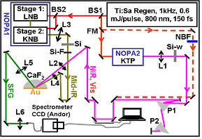
[4]. “Generation of Sub-30 fs Microjoule Mid-infrared Pulses for Ultrafast Vibrational Dynamics at Solid/Liquid Interfaces”
A. Boulesbaa, O. Isaienko, A. Tuladhar, and E. Borguet
Optics Letters, 38 (2013), 5008-5011
Abstract: We describe temporal compression of ultrabroadband, few microjoule mid-infrared (mid-IR) pulses from a noncollinear optical parametric amplifier (NOPA) employed in a sum-frequency generation (SFG) vibrational spectroscopic system, operating in total-internal-reflection geometry. The propagation of the mid-IR beam through optical materials results in a significant temporal chirp at the probed interface, which is analyzed and corrected by properly managing the total dispersion of materials introduced into the mid-IR beam path. By employing the simultaneous spatial and temporal focusing of the broadband infrared pulses at the probed interface, we achieve a sub-50-fs full width at half-maximum (FWHM) for the instrument response function, measured via SFG cross correlation of the ultrashort mid-IR pulses with an ultrashort (∼30 fs∼30 fs) near-IR pulse from a synchronized, independently tunable NOPA. From the SFG cross-correlation FWHM, we extract a sub-30-fs mid-IR pulse duration, making it a suitable SFG spectroscopic system to investigate vibrational dynamics in hydrogen-bonded systems at interfaces.
2007-2011
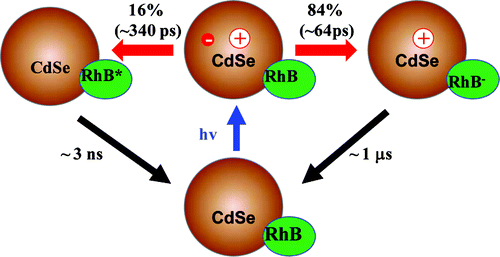
[3]. “Competition between Energy and Electron Transfer from CdSe QDs to Adsorbed Rhodamine B”
A. Boulesbaa, Z. Huang, D. Wu, and T. Lian
J. Phys. Chem. C, 114 (2010), 962-969
Abstract: Understanding the dynamics of exciton quenching in quantum dots (QDs) is essential to their potential applications, such as solar cells and biological imaging. In this work, the competition between electron and energy transfer from excited CdSe QDs to adsorbed rhodamine B (RhB) molecules was examined by time-resolved fluorescence decay, steady-state emission, and transient absorption measurements. The major pathway (84%) for exciton quenching in this system is through electron transfer to RhB, whereas ∼16% of the excitons decay by energy transfer. In a sample with ∼2−3 RhB per QD, exciton quenching occurs with an average time constant of 54 ps, and the charge-separated state has an average lifetime of 1 μs. The charge separation rate depends on the number of adsorbates attached to the QD, and the dependence can be well-described by a kinetics model that assumes a Poisson distribution of the number of adsorbates on the QDs.
[2]. “Comparison of Electron Injection Dynamics from Rhodamine B to In2O3, SnO2, and ZnO Nanocrystalline Thin Films”
J. Huang, D. Stockwell, A. Boulesbaa, J. Guo, and T. Lian
J. Phys. Chem. C, 112 (2008), 5203 -5212
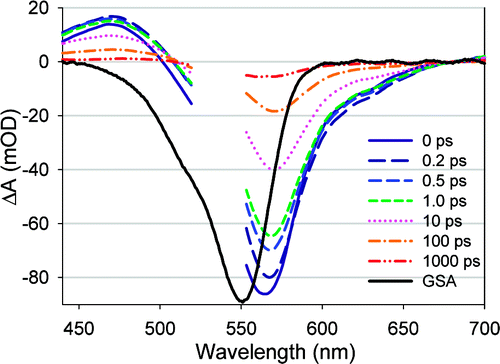
Abstract: Interfacial electron transfer (ET) dynamics from excited rhodamine B (RhB) to three semiconductor nanocrystalline thin films (In2O3, SnO2, and ZnO) was investigated to examine their dependence on semiconductors. The injected electrons in the semiconductors were directly measured by their transient absorption in the mid-IR region (∼5 μm), and the evolution of the adsorbate in its ground, excited, and cation states was monitored by its transient absorption in the visible region. The formation of the IR absorption of injected electrons correlates well with the decay of the RhB excited state, allowing an unambiguous determination of electron injection rates from the adsorbate excited state to the semiconductor nanoparticles. The recombination processes were monitored by following the decay of injected electrons and RhB cations and the recovery of the RhB molecules in the ground state. The effects of dye aggregation and excited-state quenching on the injection dynamics were also examined and were shown to be negligible under low dye coverage and excitation power density. Injection times to In2O3 and SnO2 are similar (1.2 ps) and are ∼6 times faster than to ZnO (7.0 ps). Possible reasons for the semiconductor dependent injection rates are discussed.
[1]. “Ultrafast Charge Separation at CdS Quantum Dot/Rhodamine B Molecule Interface”
A. Boulesbaa, A. Issac, D. Stockwell, Z. Huang, J. Huang, J. Guo, and T. Lian
J. Am. Chem. Soc., 129 (2007), 15132 -15133
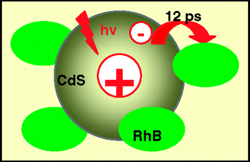
Abstract: Ultrafast dissociation of excitons in CdS quantum dots via electron transfer to adsorbed rhodamine B (RhB) molecules was demonstrated. The rate of electron transfer can be controlled by the number of adsorbates attached on the nanoparticle and transfer time as fast as 12 picoseconds was observed. The rapid and controllable charge separation in this model quantum dot−adsorbate complex provides a potential approach for separating multiple excitons before the exciton−exciton annihilation process.