

Hybrid Microelectronics Laboratory
The Hybrid Microelectronics Laboratory is located in Jacaranda Hall, Room 1101.
The lab space is approximately 1148 square feet. This is one of the newest laboratories in the department, and has been primarily used for conducting experiments and fabricating semiconductor devices for the solid state courses.
The undergraduate and graduate students benefit from hands-on-experience of present cutting-edge technology and gain the conceptual understanding of the foundation of solid state device, as well as device fabrication and applications.
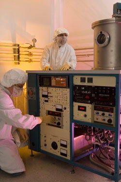
The lab is equipped with fabrication facility of front-end wafer processing using diffusion furnace for doping the semiconductor material, MA 56 mask aligner for photolithography, different sputtering units along with Kurt J. Lesker PV75 with two magnetron guns for deposition of indium tin oxide, silicon oxide, aluminum nitride and nickel.
Different characterization tools such as high frequency oscillator, four-point probe, optoelectronic test bench, curve tracer, parametric analyzer and analytical instrument are available to characterize the semiconductor device wafer level.
In 2005 to 2008, the DoD awarded research grant of half million dollars and the OPFET device has been successfully developed in this laboratory under Dr. Somnath Chattopadhyay supervision. In 2011, the research on graphene FET has been started under the supervision of Dr. Somnath Chattopadhyay to diversify the microelectronics lab to nanotechnology lab for developing new generation of biosensors.
In 2012, Dr. Chattopadhyay received half million dollars of research grant from the DoD to develop the optically triggered silicon carbide/gallium nitride (SiC/GaN) MESFET in the microelectronics laboratory to be used for advanced actuator system for military and commercial aviation (Boeing).